IR Cameras & Pyrometers for Semiconductor Industry
Accurate Temperature Measurement for Fabrication and Testing
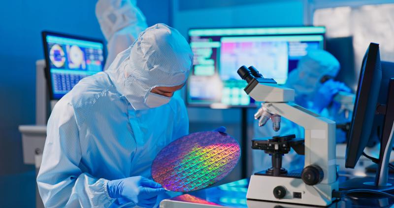
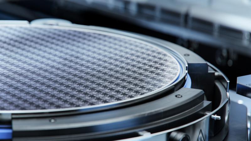
The Importance of IR Non-Contact Temperature Measurement in the Semiconductor Industry
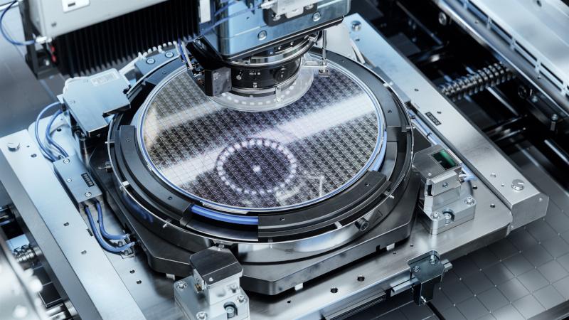
Infrared (IR) temperature measurement is essential in the semiconductor industry for optimizing various high-precision processes. Accurate temperature control is crucial in Physical Vapor Deposition (PVD) and Chemical Vapor Deposition (CVD), where precise thermal management ensures the uniform coating of semiconductor wafers. IR cameras and pyrometers provide non-contact temperature readings, allowing for real-time monitoring and adjustments during these deposition processes, which are critical for achieving high-quality thin films and coatings.
In polysilicon production and rapid thermal annealing, IR temperature measurement helps maintain optimal conditions for the thermal processing of semiconductor materials. Accurate temperature control prevents defects and ensures the uniformity of the polysilicon layers, which is vital for the performance and reliability of semiconductor devices.
During lithography, IR sensors monitor and control the temperature of exposure systems, which directly impacts pattern accuracy and device performance. In the strip and clean process, IR technology helps manage temperatures during the removal of photoresist and other materials, ensuring effective and consistent processing.
Overall, integrating IR temperature measurement into semiconductor manufacturing enhances process efficiency, product quality, and operational reliability, making it a critical tool for modern semiconductor production.
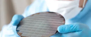
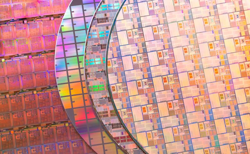
Semiconductors Applications


Main Challenges of Non-Contact Temperature Measurement in the Semiconductor Industry
Infrared (IR) non-contact temperature measurement presents specific challenges in the semiconductor industry. One major challenge is emissivity variation across different semiconductor materials. In processes like Physical Vapor Deposition (PVD) and Chemical Vapor Deposition (CVD), the varying emissivity of substrates and thin films can affect the accuracy of IR temperature readings. Proper calibration is essential to account for these differences, as inaccuracies can lead to suboptimal process control and compromised quality.
Another challenge involves thermal gradients and temperature uniformity in high-precision processes such as polysilicon production and rapid thermal annealing. Semiconductor wafers and components often experience uneven heating, which IR sensors must detect accurately. The complexity of managing these gradients requires advanced IR technology capable of high-resolution thermal imaging and precise temperature monitoring to maintain consistent quality.
Ambient heat interference and reflective surfaces also impact the accuracy of IR measurements. In processes like lithography and the strip and clean process, managing thermal interference from surrounding equipment and reflective surfaces is critical. Effective shielding and careful sensor placement are necessary to ensure reliable temperature readings and process integrity.
Benefits of Using IR Non-Contact Temperature Measurement in Semiconductor Manufacturing
Despite these challenges, IR non-contact temperature measurement offers substantial benefits in enhancing quality in the electronics industry. In Physical Vapor Deposition (PVD) and Chemical Vapor Deposition (CVD), IR sensors provide precise thermal monitoring, ensuring uniform coating of semiconductor wafers. This precision helps in achieving the desired film thickness and quality, directly impacting the performance and reliability of electronic components.
For polysilicon production and rapid thermal annealing, IR technology ensures optimal temperature control during critical thermal processing. Accurate temperature management prevents defects and inconsistencies in polysilicon layers, which are crucial for producing high-quality semiconductor devices. This leads to improved product yield and performance.
Lithography and strip and clean processes also benefit from IR temperature measurement. During lithography, maintaining the correct temperature in exposure systems ensures pattern accuracy and reduces defects. In the strip and clean process, IR sensors help manage temperatures to effectively remove photoresists and other materials, ensuring consistent processing and high-quality outcomes.
Applications and Efficiency Gains
IR non-contact temperature measurement delivers significant efficiency gains across various electronics manufacturing applications. In PVD and CVD, IR cameras provide real-time thermal data, allowing for immediate adjustments and optimization of deposition processes. This leads to enhanced process efficiency and product consistency.
In polysilicon production and rapid thermal annealing, accurate temperature control helps in achieving uniform thermal profiles, reducing waste, and improving production throughput. For lithography, real-time thermal monitoring ensures that exposure systems operate within optimal temperature ranges, enhancing pattern fidelity and device performance.
Overall, integrating IR technology into electronics manufacturing processes contributes to higher product quality, reduced operational costs, and more efficient production practices. By offering precise temperature control and real-time monitoring, IR sensors play a crucial role in optimizing electronics production and achieving superior manufacturing outcomes.
What Is the Right Solution for My Needs?
Click here to find the product that suits your demands.

Talk to us about your IR Temperature Measurement Requirements
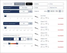
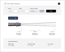
There are over 300 different pyrometer variants to choose from in the Optris infrared pyrometer portfolio each optimized for material, spot size, distance from the target, and environmental conditions. Fortunately, there is a trained engineer to phone or chat with to guide you through the process of choosing the perfect infrared sensor for your application.
The same support is available for the extensive IR camera product line.